成功加入购物车
潘森 著 / 科学出版社 / 2007-01 / 平装
售价 ¥ 75.00
品相 九五品
延迟发货说明
上书时间2025-06-07
卖家超过10天未登录
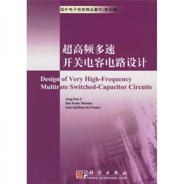
国外电子信息精品著作:超高频多速开关电容电路设计
《超高频多速开关电容电路设计(影印版)》是一本专业性很强的书,《超高频多速开关电容电路设计(影印版)》以具体实例为依托,详细阐述了作者所设计的一款性能优越、用途广泛的高频开关电容电路,并对该电路设计中所涉及到的模拟CMOS集成电路设计的很多重要问题进行讲解。其实这些问题并不仅仅出现于《超高频多速开关电容电路设计(影印版)》所介绍的这种电路类型,而是在模拟集成电路设计中经常会遇到的一些问题,所以该书的参考价值可以扩展到更大的领域。更难能可贵的是作者所设计的这款电路的优越性能得到了实际芯片测试的验证,亦即增加了《超高频多速开关电容电路设计(影印版)》的权威性。
PrefaceAcknowledgmentListofAbbreviationsListofFiguresListofTables1INTRODUCTION1.High-FrequencyIntegratedAnalogFiltering2.MultirateSwitched-CapacitorCircuitTechniques3.Sampled-DataInterpolationTechniques4.ResearchGoalsandDesignChallenges2IMPROVEDMULTIRATEPOLYPHASE-BASEDINTERPOLATIONSTRUCTURES1.Introduction2.ConventionalandImprovedAnalogInterpolation3.PolyphaseStructuresforOptimum-classImprovedAnalogInterpolation4.MultirateADBPolyphaseStructures4.1CanonicandNon-CanonicADBRealizations4.2SCCircuitArchitectures5.Low-SensitivityMultirateIIRStructures5.1MixedCascade/ParallelForm5.2Extra-RippleIIRForm6.Summary3PRACTICALMULTIRATESCCIRCUITDESIGNCONSIDERATIONS1.Introduction2.PowerConsumptionAnalysis3.Capacitor-RatioSensitivityAnalysis3.1FIRStructure3.2IIRStructure4.FiniteGain&BandwidthEffects5.Input-ReferredOffsetEffects6.PhaseTiming-MismatchEffects6.1PeriodicFixedTiming-SkewEffect6.2RandomTiming-JitterEffects7.NoiseAnalysis8.Summary4GAIN-ANDOFFSET-COMPENSATIONFORMULTIRATESCCIRCUITS1.Introduction2.AutozeroingandCorrelated-DoubleSamplingTechniques3.AZandCDSSCDelayBlockswithMismatch-FreeProperty3.1SCDelayBlockArchitectures3.2GainandOffsetErrors-ExpressionsandSimulationVerification3.3Multi-UnitDelayImplementations4.AZandCDSSCAccumulators4.1SCAccumulatorArchitectures4.2GainandOffsetErrors-ExpressionsandSimulationVerification5.DesignExamples6.SpeedandPowerConsiderations7.Summary5DESIGNOFA108MHzMULTISTAGESCVIDEOINTERPOLATINGFILTER1.Introduction2.OptimumArchitectureDesign2.1MultistagePolyphaseStructurewithHalf-BandFiltering..2.2Spread-ReductionScheme2.3Coefficient-SharingTechniques3.CircuitDesign3.1lst-Stage3.22nd-and3rd-Stage3.3DigitalClockPhaseGeneration4.CircuitLayout5.SimulationResults5.1BehavioraISimulations5.2Circuit-LevelSimulations6.Summary6DESIGNOFA320MHZFREQUENCY-TRANSLATEDSCBANDPASSINTERPOLATINGFILTER1.Introduction2.PrototypeSystem-LevelDesign2.1Multi-notchFIRTransferFunction2.2Time-InterleavedSerialADBPolyphaseStructurewithAutozeroing3.PrototypeCircuit-LevelDesign3.1AutozeroingADBandAccumulator3.2High-SpeedMultiplexer3.3OverallSCCircuitArchitecture3.4TelescopicopampwithWide-SwingBiasing3.5nMOSSwitches1363.6NoiseCalculation3.7I/0Circuitry3.8LowTiming-SkewClockGeneration4.LayoutConsiderations4.1DeviceandPathMatching4.2SubstrateandSupplyNoiseDecoupling4.3Shielding4.4FloorPlan5.SimulationResults5.1OpampSimulations5.2FilterBehavioralSimulations5.3FilterTransistor-LevelandPost-LayoutSimulations6.Summary7EXPERIMENTALRESULTS1.Introduction2.PCBDesign2.1FloorPlan2.2PowerSuppliesandDecoupling2.3BiasingCurrents2.4InputandOutputNetwork3.MeasurementSetupandResults3.1FrequencyResponse3.2Time-DomainSignalWaveforms3.3One-ToneSignalSpectrum3.4Two-ToneIntermodulationDistortion3.5THDandIM3vs.InputSignalLevel3.6NoisePerformance3.7CMRRandPSRR4.Summary8CONCLUSIONSAPPENDIX1TIMING-MISMATCHERRORSWITHNONUNIFORMLYHOLDINGEFFECTS1.SpectrumExpressionsforIU-ON(SH)andIN-CON(SH)1.1IU-ON(SH)1.2IN-CON(SH)2.ClosedFormSINADExpressionforIU-ON(SH)andIN-CON(SH)2.1IU-ON(SH)2.2IN-CON(SH)3.ClosedFormSFDRExpressionforIN-CON(SH)systems4.SpectrumCorrelationofIN-OU(IS)andIU-ON(SH)APPENDIX2NOISEANALYSISFORSCADBDELAYLINEANDPOLYPHASESUBFILTERS1.OutputNoiseofADBDelayLine2.OutputNoiseofPolyphaseSubfilters2.1UsingTSIInputCoefficientSCBranches2.2UsingOFRInputCoefficientSCBranchesAPPENDIX3GAIN,PHASEANDOFFSETERRORSFORGOCMFSCDELAYCIRCUITIANDJ1.GOCMFSCDelayCircuitI2.GOCMFSCDelayCircuitJ
展开全部
配送说明
...
相似商品
为你推荐
开播时间:09月02日 10:30